Noriaki Toyoda
Professor | Ph.D. in Engineering
Electrical and Electronic Engineering Course
Nanoprocess Research Group
Electromagnetism and electric circuits pose persistent conceptual hurdles for many students, and Toyoda's teaching focuses closely on the specific points where learners tend to stumble, using mathematics to show how seemingly complex problems in electrical, electronic, and information engineering can be simplified. His research pursues distinctive nanoprocessing technologies, spanning the discovery of new physical principles, the development of original equipment, and their application to practical engineering challenges.
Development of New Nanoprocessing Equipment
What students can learn
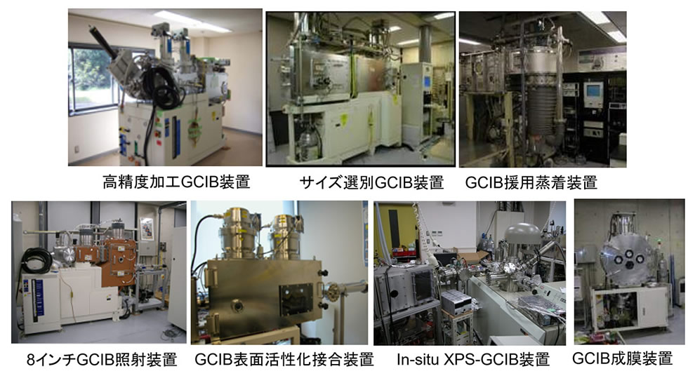
In this laboratory, students design and construct their own equipment to realize novel processing principles based on gas clusters, developing practical skills in CAD design, control programming, materials selection, and structural strength design.
New processing technologies rarely emerge from equipment that can simply be purchased off the shelf. This research instead builds, modifies, and refines equipment in-house, cultivating the ability to identify problems and resolve them independently. Collaborative projects with leading semiconductor-related companies in Japan and abroad expose students to cutting-edge technology and let them acquire research methods through direct, hands-on experience.
Development of New Nanostructure Formation Methods
What students can learn
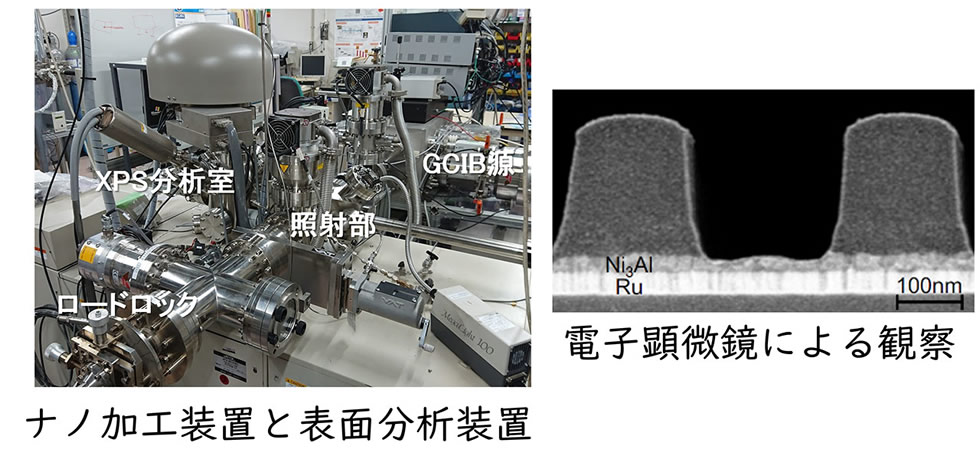
Here, students acquire analytical and measurement techniques such as electron microscopy and spectroscopy, while also applying atomistic simulations to understand the physical processes underlying nanoprocessing.
This research explores nanostructure formation methods using clusters composed of thousands of gas molecules. To investigate what happens when these clusters strike a surface, the group links nanoprocessing equipment directly with surface-analysis instruments and observes surface states using X-rays. Insight into surface properties and reactions helps inform the development of new nanoscale processing methods.