Akira Heya
Professor | Ph.D. in Materials Science
Materials Design Course
Field of Materials Design
Semiconductors, often called the "rice of industry," underpin our information society. The Semiconductor and Biomaterials Research Group pursues the development of new semiconductor materials and semiconductor devices based on novel operating principles, with the aim of realizing a sustainable society. In the third-year undergraduate course "Semiconductor Engineering," lectures cover the structure, constituent materials, and operating principles of fundamental semiconductor devices such as diodes and transistors. In the graduate course "Semiconductor Thin-Film Engineering," students examine surface, vacuum, and thin-film technologies in detail, along with applications such as solar cells, thin-film transistors, and displays.
Development of Next-Generation Semiconductor Materials and Device Applications Using Atomic Hydrogen and Nitrogen
What students can learn
Students learn how chemical reactions proceed under specialized conditions and acquire techniques for developing novel materials. They also come to understand the operating principles of semiconductor devices and gain the knowledge and skills needed to improve device performance.
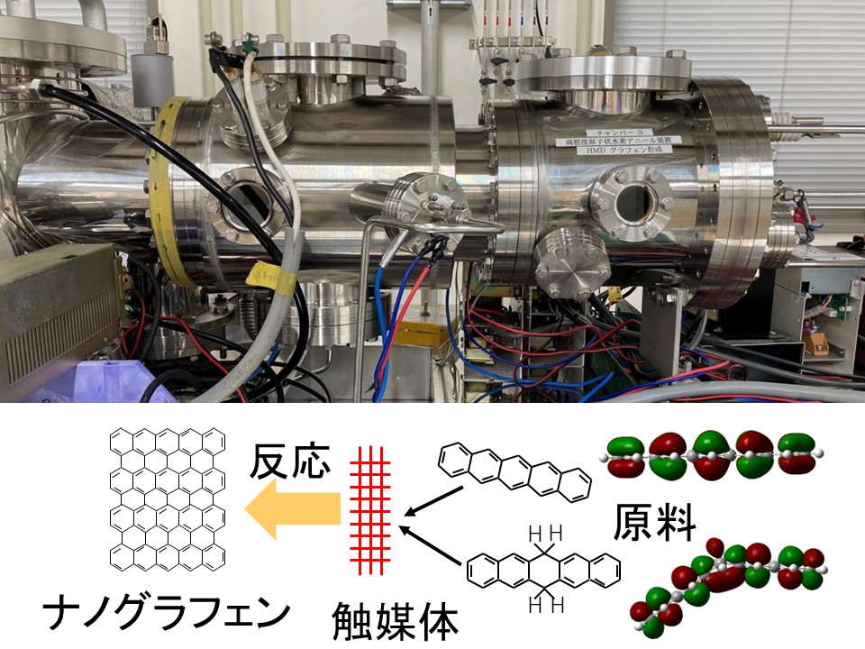
This research controls the polymerization of organic materials to develop new semiconductor materials capable of replacing conventional silicon. It also advances techniques for fabricating graphene nanoribbons from pentacene and hydrogen, and for reducing and nitrogen-doping graphene oxide using atomic hydrogen and nitrogen to produce nitrogen-doped graphene. These techniques aim to realize the low-power, high-speed semiconductor devices that underpin the information society.
Development of Novel Semiconductor Processes Using Atomic Hydrogen and Nitrogen, and Contributions to a Hydrogen-Based Society
What students can learn
Students learn the fundamentals of vacuum technology and develop the ability to understand, at the atomic level, the properties of hydrogen and ammonia—both promising next-generation energy carriers. They also examine the current state and challenges of semiconductor manufacturing processes and build the capacity to develop new fabrication processes.
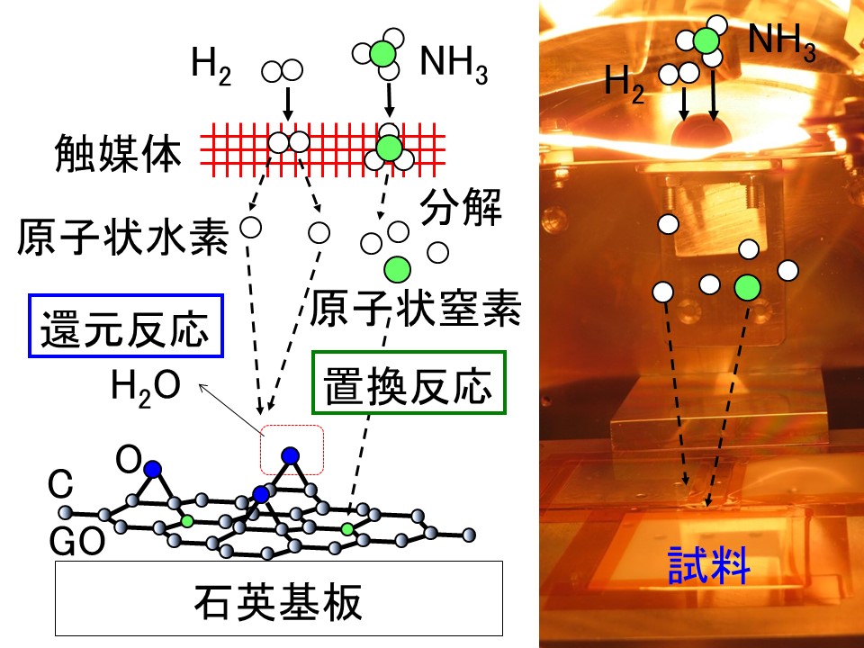
This research develops novel semiconductor processes that employ atomic hydrogen generated by decomposing hydrogen gas, contributing to a sustainable information society. Because atomic hydrogen is highly reactive and known to degrade materials, this work clarifies the underlying degradation mechanisms and designs materials resistant to such degradation. In addition, by elucidating the reactions between various materials and atomic nitrogen generated from decomposed ammonia gas, this research contributes to the realization of a safe and sustainable society.