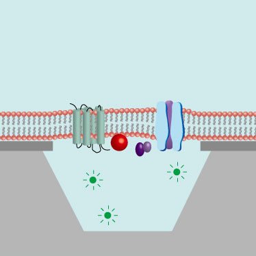
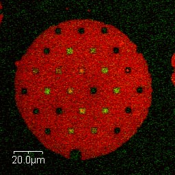
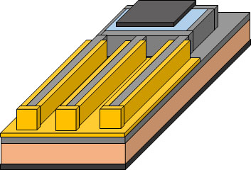
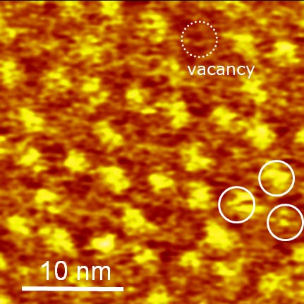
We aim to create new devices by fusing a wide range of technologies such as materials science, surface science, semiconductor devices, nanotechnology, and nanobiotechnology. Our goal is to establish basic technologies that contribute to health and medical applications, such as early diagnosis of diseases and high-throughput screening in drug discovery.
当研究室は,材料工学,表面科学・半導体デバイス・ナノテクノロジー・ナノバイオテクノロジー等の幅広い技術を融合し,新しいデバイスの創生を目指しています. 同時に,疾病の早期診断や創薬におけるハイスループットスクリーニング等,健康・医療応用にも貢献する基盤技術の確立につなげていきます.
Upcoming Presentation
-
AFMPD'26(2026.7.7-11)
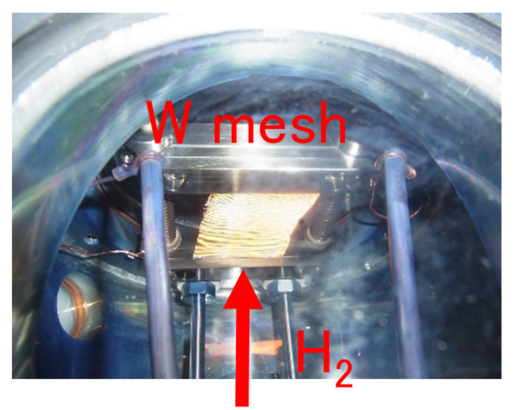
- "Characteristics of DLC-Coated QCM Sensor for Atomic Hydrogen Detection"
A. Heya, S. Niihara, I. Tanaka, K. Sumitomo -
ACSIN-16/ICSPM34(2026.10.19-23)
Link
Contact
Himeji Campus for Engineering, University of Hyogo,
2167 Shosha, Himeji, Hyogo 671-2280, Japan
E-mail: sumitomo@eng.u-hyogo.ac.jp